High Magnification, High Resolution Calibration Reference and Traceable Standard for AFM, SEM, Auger and FIB
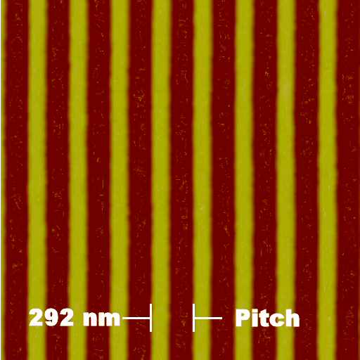
precision, holographic pattern featuring high accuracy, usability and stability. Its moderate ridge height makes it convenient for AFM. This specimen provides excellent contrast in back-scatter as well as secondary electron imaging. It provides accurate calibration for high resolution, nanometer-scale measurements.
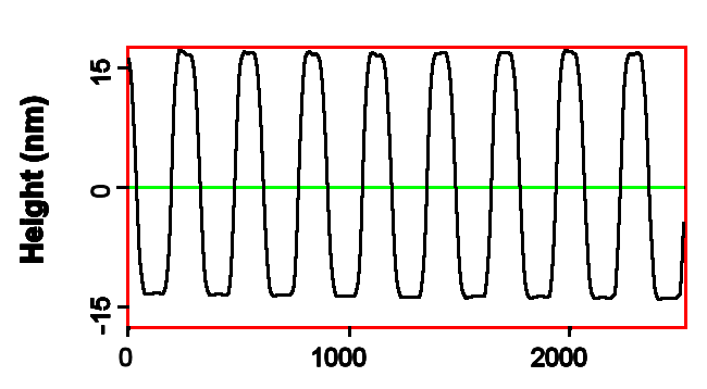
Period: 292 nm pitch, one-dimensional grating. Accurate to +/- 1% (3 standard deviations).
Surface: Titanium lines on Silicon wafer, 3 x 4mm. Line height (about 30 nm) and line width (about 130 nm) are not calibrated.
Characteristics: High contrast, excellent edge definition. In AFM, use in contact, intermittent contact (TappingModeTM ) and other modes with image sizes from 500 nm to 20 mm. Use SEM beam voltages from under 1 kV to 30 kV. Useful from 5,000x to over 200,000x. In Auger and Focused Ion Beam (FIB), use similar conditions as for SEM. Available unmounted to accommodate all SEM stages. For AFM, available unmounted or mounted on 12 mm steel disks.
Usability: the calibrated pattern covers the entire chip. There is sufficient usable area to make tens of thousands of measurements without reusing any areas altered or contaminated by previous scans.
Model 301BE. This Calibration Reference specimen comes with a non-traceable, manufacturer’s certificate. This states the average period, based on batch measurements.
Model 292UTC. This Traceable, Certified Standard is a select grade. Each standard is individually measured in comparison with a similar specimen calibrated at PTB. (PTB, Physikalisch-Technischen Bundesanstalt, is the German counterpart of NIST.) The uncertainty of single pitch values is typically +/- 2 nm (95% confidence interval). Multi-pitch measurements provide the usual square-root of N improvement in precision. Learn about the difference betwen a traceable calibration STANDARD and an ordinary calibration REFERENCE specimen.


