Atomic Force Microscopy is a powerful tool for the Electronics industry. Not only is it used to characterize the materials themselves, but it is used to help develop the tools for the processing of electronic materials and the manufacture of electronic components.
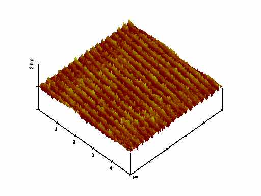
The high component densities of modern semiconductor chips requires extremely smooth and homogeneous surfaces. Atomic Force Microscopes allow direct measurement of surface roughness down to the atomic level. The AFM can measure individual atomic steps on superpolished surfaces.


Smaller components, narrower trace widths, and higher component densities require optics that can focus shorter and shorter wavelengths of light, extending even past ultraviolent into the X-ray regime. X-rays can be focused using grazing-incidence mirrors but this requires extremely smooth surfaces. The same atomic-level surface roughness measurements used for materials can also be used for optical materials, the same way they can in semiconductor wafers.
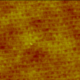
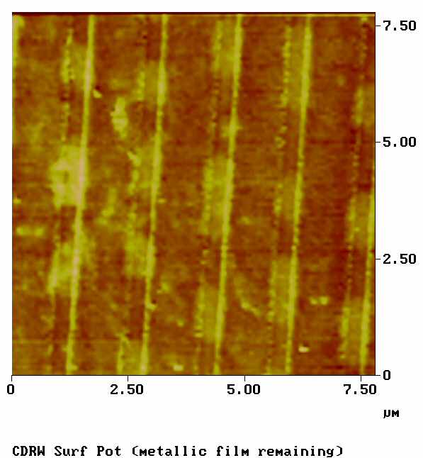
But Atomic Force Microscopes can do so much more than inspect wafers and optics for smoothness. Techniques such as Magnetic and Electric Force Imaging and Scanning Kelvin/Surface Potential imaging can detect and map differences in the surface.

Going beyond these basic techniques, more advanced techniques such as Conductive AFM (CAFM or C-AFM), Scanning Spreading Resistance Microscopy (SSRM), Tunneling Atomic Force Microscopy (TUNA), and others give a deeper understanding of surface character allowing for quicker development times with fewer pitfalls and producing a better quality product.


