
Atomic Force Microscopy
Introduction
The Atomic Force Microscope (AFM) is being used to solve processing and materials problems in a wide range of technologies affecting the electronics, telecommunications, biomedical, chemical, automotive, aerospace, and energy industries. The materials under investigation include thin and thick film coatings, ceramics, composites, glasses, synthetic and biological membranes, metals, polymers, and semiconductors. The AFM is being applied to studies of phenomena such as abrasion, adhesion, cleaning, corrosion, etching, friction, lubrication, plating, and polishing. The real-world examples presented on our web site indicate the breadth of AFM applications for problem solving; yet they represent only a fraction of our experience at Advanced Surface Microscopy.
Technical Capabilities
AFM images show critical information about surface features with unprecedented clarity. The AFM can examine any rigid surface, either in air or with the specimen immersed in a liquid. “Minor” (and major) differences between “smooth” surfaces are shown dramatically. On one hand, the AFM can resolve very tiny features, even single atoms, that were previously unseen. On the other hand, the AFM can examine a field of view larger than 125 microns (0.005 inch), so that you can make comparisons with other information, e.g. features seen in the light microscope or hazes seen by eye. The AFM can also examine rough surfaces, since its vertical range is more than 5 microns. Our analytical reports of AFM results include three-dimensional images and quantitative data analysis (such as feature sizes, surface roughness and area, and cross-section plots), integrated and interpreted in the context of your problem.
Large samples fit directly in the microscope without cutting. We can examine any area on flat specimens up to 8″ (20 cm) in diameter and up to 0.5″ (12.7 mm) thick. We have designed custom adapters to accommodate SEM stubs, microtomed blocks, metallurgical mounts, and other odd shapes and sizes (up to 1.5″ thick and 42″ wide). We can quickly find and document the location of interest using the built-in optical microscope (with magnification up to 2000x). For comparative studies using different probes and scanning modes, we can find the spot within one micron.
How the AFM makes a 3D image

In contact mode, a tiny stylus gently contacts the specimen. As the XYZ translator scans either the specimen or the stylus horizontally in a raster pattern (XY), the stylus rides up and down the surface hills and valleys. The deflection of the stylus is registered by the laser/photodiode sensor and the XYZ translator adjusts stylus or specimen (depending on microscope) up or down (Z) to restore the stylus to its original orientation. The computer stores the vertical position at each point and assembles the image.
Another method is TappingMode
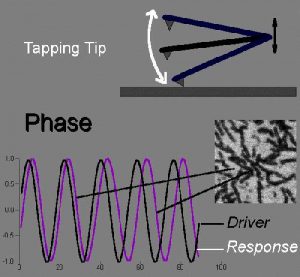
For image display, we select the vertical (Z) and horizontal (XY) ranges independently, to best present the surface structure. Using “dual magnification,” the AFM combines the wide field view of a Scanning Electron Microscope (SEM) with vertical resolution which exceeds that of a Transmission Electron Microscope (TEM). The ratio of the vertical to horizontal magnification can be very large (1000 or more) to allow easy perception of differences between very smooth surfaces.
Aluminum Can Coating
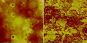
Topographic results can be enhanced by simultaneously using other modes of AFM data capture, such as phase imaging. In the left image (above), we see the many interesting surface features of the coating. When combined with the phase image (right), we can now tell which features are of similar chemical composition. This allows determining whether surface features may be the result of a residue or specific chemical component, or whether the surface is homogeneous.
See what you’ve been missing
In addition to its superior resolution, the AFM has these key advantages:
- Compared with Scanning Electron Microscopes (SEM), the AFM provides extraordinary topographic contrast, direct height measurements and unobstructed views of surface features (no coating is necessary).
- Compared with Transmission Electron Microscopes, 3-dimensional AFM images are obtained without expensive sample preparation and yield far more complete information than the 2-dimensional profiles available from cross-sectioned samples.
- Compared with Optical Interferometric Microscopes (Optical Profilers), the AFM provides unambiguous measurement of step heights, independent of reflectivity differencences between materials.
Contaminants on Glass
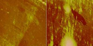
Another mode of operation which can be useful when combined with topography is friction imaging. In the height image above (left), there are several areas where the topography appears higher and rougher than the bulk surface. When combined with a friction image (right), we see that there is a contaminant on the surface which appears dark in the image. Therefore the contaminant has a lower coefficient of friction than the underlying surface. This can be helpful in determining the source of the contaminant.
Exotic invention or practical tool?
The Scanning Tunneling and Atomic Force Microscopes are well-known due to their extraordinary capability of imaging atoms using a simple mechanism.
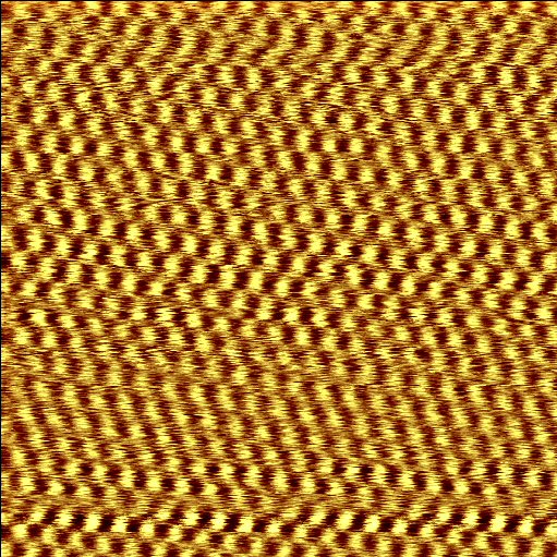
highly ordered pyrolitic graphite (HOPG).
However, atomic resolution is usually not needed to solve most problems in development and manufacturing. As a result, many scientists mistakenly regard these new microscopes as more exotic than practical.
Both the AFM and STM make 3-Dimensional images of solid surfaces, but the AFM has much broader applications. The reason for this is that the AFM uses a universal sensing mechanism (repulsive and attractive mechanical forces), whereas the STM uses an electrical signal, which requires that the surface be at least somewhat conductive.
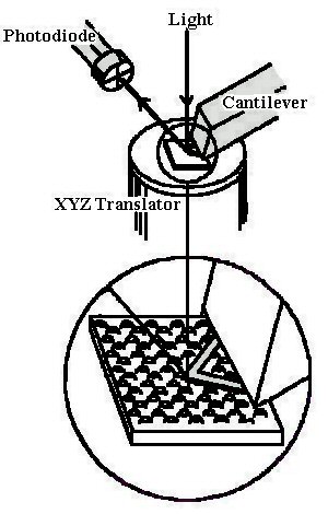
scanned over the surface, the cantilever
deflects upward, changing the angle
of the beam of light reflected to the
split photodiode. This allows the tip
to accurately track the surface.
Using the extraordinary height sensitivity and wide scan capabiity of the AFM, we can easily answer simple but important questions about surfaces and surface features including:
- Is a contaminant present
- Is a feature a pit or a peak
- How tall is it
- What is the grain size of a coating
- How rough is the surface
- Is a coating continuous or broken
Answering these questions and others like them provides several applications which have practical value for a diverse group of industries. We provide several examples.
AFM Image of Aluminum Foil
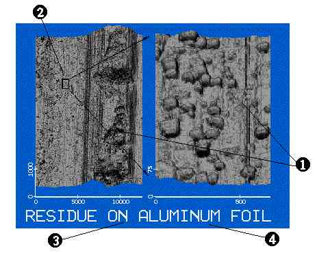
AFM images of aluminum foil show many shallow bumps (5-25 nm high), which cover features associated with the rolling process (such as large tears and fine scratches). It is evident that the bumps are depositied after the foil emerges from the rollers. We believe this contaminant is a non-volatile residue derived from the rolling lubricant. The ability to detect the amount of residue on the foil surface helps metallurgists improve product clenliness.
Magnetic Recording Heads
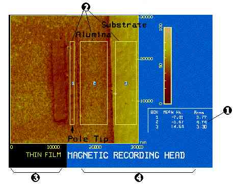
showing height difference between different
elements of the head.
High Density Magnetic Storage depends on precise fabrication of the recording head. Thin film heads are fabricated by deposition of alumina and ferrite layers on an alsimag substrate, followed by cross sectional polishing to expose teh ferrite pole tips. The layers and interfaces are crisply defined in AFM images and we can determine the critical height information.
Optical Disk Stampers
are the data marks. THe smaller bumps on and around them are
roughness features, probably grains, of nickel.
AFM images of optical disk stampers show the general shape of the data bumps, including the hegith, width, and wall slopes, as well as flaws and the fine grain structure of the Ni surface. We started working with people producing CD’s but as manufacturers develop each new generation of media, the tolerances become tighter and more critical, increasing the need for precise and accurate measurement. To assist with this, we developed the measurement software DiscTrack Plus.