The Scanning Tunneling Microscope originally gained attention as a simple device for imaging atoms. From that exotic beginning, there has grown a family of Scanning Probe Microscopes, of which the Atomic Force Microscope (AFM) is the most common. Various versions of these instruments operate in air, in liquid, and in vacuum. They record 3-dimensional topography, magnetic and electric fields, friction, adhesion, stiffness, optical spectra, and more.
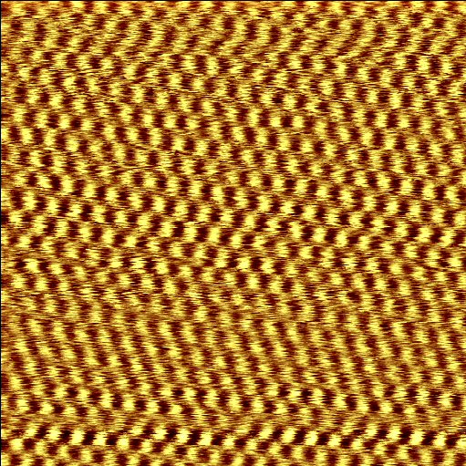
highly ordered pyrolitic graphite (HOPG).
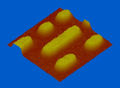
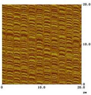
image of data on a magnetic hard disk.
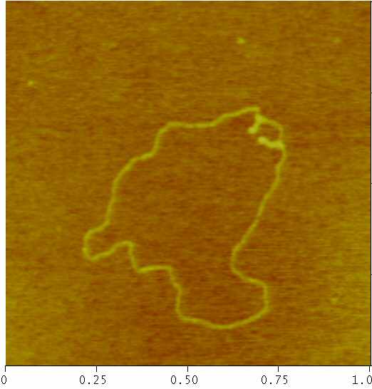
Composite surfaces of industrial interest may be created either deliberately (examples include: microfabrication of thin-film recording heads and polymer processing) or accidentally (contaminants on or defects in the surface). TappingModeTM/Phase images can map the material domains with spatial resolution down to 10 nm. Such images can be a powerful aid in process control.
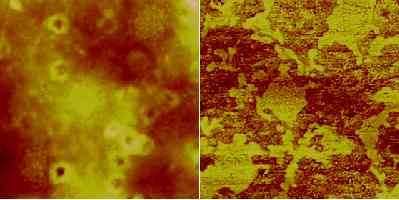
Phase images show the mechanical phase of the tapping tip relative to the drive signal which oscillates the cantilever. The phase image supplements the ordinary height image and often provides unique contrast related to material differences in stiffness and adhesion.
Nano-indentation and Nano-scratching have been developed to provide further information about stiffness and wear resistence with high sensitivity and spatial resolution.
In addition, with proper calibration specimens and our calibration correction software, standard, general use, AFM’s can make accurate and highly precise measurements.
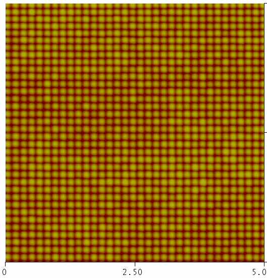

of calibration specimen without calibration
correction. (Standard factory calibration)

specimen with calibration correction. (Special high-accuracy calibration using our software)


