
70-1D/70-1DUTC – SOLD OUT
Notice: Although this product is not available for sale, reference information remains on the site.
Details
- Applications: AFM, SEM, Auger, FIB
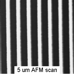
- Pattern: parallel ridges
- Approximate Pitch1: 70 nm
- Material: SiO2 on Si
- Mounting: Unmounted, On 12 or 15 mm Steel Disk, or on SEM Stub (extra charge)
- Remarks: Use Contact or Tapping mode AFM. Works well in SEM
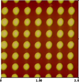
150-2D/150-2DUTC
Details
- Applications: AFM, SEM, Auger, STM
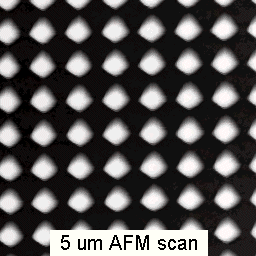
- Pattern: Array of rounded bumps
- Approximate Pitch1: 144 nm
- Material: Si bumps on Si
- Mounting: Unmounted, on 12 or 15 mm Steel Disk, or on SEM Stub (extra charge)
- Remarks: use contact or tapping mode. Works well in SEM.
150-1D/145TC
Details
- Applications: AFM,SEM2, TOF-SIMS, Auger, Surface Potential, other material contrast techniques. NSOM’s Super Resolution Optical Microscopy
- Pattern: Parallel Ridges
- Approximate Pitch1: 144 nm
- Material: Al lines on Glass
- Mounting: Unmounted or on 12 or 15 mm steel disk
- Remarks: use contact or tapping mode..
750-HD
Details
- Applications: AFM,SEM, STM
- Pattern: Array of flat bumps
- Approximate Pitch1: X 750, Z 100 nm
- Material: Ni
- Mounting: Unmounted
- Remarks: High Durability: TappingMode, Contact Mode, STM, Liquid, High Temperature
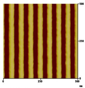
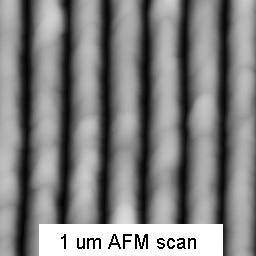
300-1D
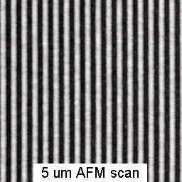
Details
- Applications: AFM, SEM
- Pattern: Parallel Ridges
- Approximate Pitch1: 288 nm
- Material: W-coated Photoresist on Si
- Mounting: 12 or 15 mm steel disk
- Remarks: use contact or TappingMode.
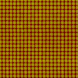
300-2D
Details
- Applications: AFM, SEM
- Pattern: Array of posts
- Approximate Pitch1: 297 nm
- Material:Al bumps on Si
- Mounting: 12 or 15 mm steel disk
- Remarks: use contact or TappingMode.
301BE/292UTC
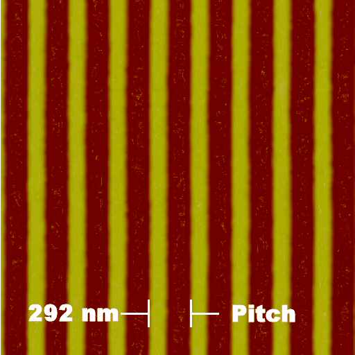
Details
- Applications: AFM, SEM, TOF-SIMS, Auger, Surface Potential, other material contrast techniques
- Pattern: Parallel Ridges
- Approximate: Pitch: 292 nm
- Material: Ti lines on Si
- Mounting: unmounted, on steel disk, or on an SEM stub (extra charge)
- Remarks: use contact or tapping mode. Works well in SEM SEI and BEI modes.
700-1D/700-1DUTC
Details
- Applications: AFM, SEM
- Pattern: Parallel Ridges
- Approximate Pitch1: 700 nm
- Material: W coated photoresist on Si.
- Mounting: 12 or 15 mm steel disk
- Remarks: use contact or tapping mode.
700-2D
Details
- Applications: AFM, SEM
- Pattern: Array of Posts
- Approximate Pitch1: 700 nm
- Material: W coated Photoresist on Si.
- Mounting: 12 or 15 mm steel disk
- Remarks: use contact or tapping mode.
PT
Details
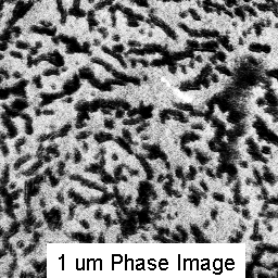
- Applications: AFM Phase Imaging
- Pattern: random hard and soft domains as small as 10 nm
- Approximate Pitch: N/A
- Material: Polymer.
- Mounting: 15 mm steel disk
- Remarks: Test resolution and build confidence in phase imaging.
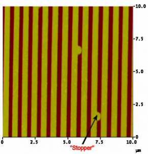
NanoChannel Array with Stopper, 751-HD
Details
- Applications: AFM, nanomechanics, nanofluidics
- Pattern: array of ridges with occasional bulges (“stoppers”)
- Approximate Pitch1: n/a. Channel width about 370 nm, depth about 180 nm
- Material: Ni.
- Mounting: unmounted, see data sheet for details
- Remarks: Confine materials in channel. Use ridges as NanoAnvil in 3-point bend test.
Priced for use as disposable substrate. Not intended as a calibrator.
We also sell traceable calibration standards
See an example of long-term calibration drift
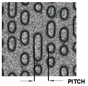
Sample Dimension and Pattern Orientation.
Traceable Calibration is now available for the 70-1D, 301BE, 150-2D, and 150-1D specimens, as models 70-1DUTC, 292 UTC, 150-DUTC, and 145 TC. This helps you achieve higher quality and meet ISO-9000 and 14000 requirements. Learn about the difference between a traceable calibration STANDARD and an ordinary calibration REFERENCE specimen.
What does traceability mean?
The calibration certificate for ordinary specimens gives an average pitch value based on batch measurements. In contrast, the certificate of traceable calibration reports the average pitch value and the uncertainty of single pitch values, based on individual measurements of the actual specimen and the measurements are traceable to the international meter. Our traceability path for 70-1DUTC is via NIST. Our traceability path for 150-2DUTC, 145TC, 292UTC, and 700-1DUTC is via PTB, the German counterpart of NIST. This is equivalent to NIST traceability, based on a mutual recognition agreement for nanoscale measurements among NIST, PTB, and other leading national measurement labs.
Specimens can be gold coated by user for STM. Sorry, no warranty or refund after you modify the specimen.
Specimens available unmounted, mounted on steel disks, or mounted on SEM mounts.
Calibration Specimen Details
| Application | Product | Pattern | Approx. Pitch1 (nm) | Material | Mounting | Remarks |
|---|---|---|---|---|---|---|
| AFM, SEM4, Auger, FIB | 70-1D (out of stock) and 70-1DUTC | parallel ridges | 70 | SiO2 on Si | unmounted, on steel disk or on an SEM stub (extra charge) | Use contact or tapping mode. Works well in SEM |
| AFM, SEM4, Auger, STM3 | 150-2D and 150-2DUTC | Array of rounded bumps | 144 | Al on Si | use contact or tapping mode. Works well in SEM SEI and BEI modes | use contact or tapping mode. Works well in SEM SEI and BEI modes |
| AFM,SEM2, TOF-SIMS, Auger2, Surface Potential, other material contrast techniques. NSOM5. | 150-1D and 145TC | Parallel ridges | 144 | Al lines on Glass | unmounted or on steel disk | use contact or tapping mode. |
| AFM, SEM4, TOF-SIMS, Auger, Surface Potential, other material contrast techniques. | 301BE and 292UTC | parallel ridges | 292 | Ti lines on Si | unmounted, on steel disk, or on an SEM stub (extra charge) | use contact or tapping mode. Works well in SEM SEI and BEI modes |
| AFM, SEM | 300-1D | Parallel ridges | 288 | W-coated Photoresist on Si | 15 mm steel disk | use contact or TappingMode. |
| AFM, SEM | 300-2D | Array of Posts | 297 | Al bumps on Si | 15 mm steel disk | use contact or TappingMode |
| AFM, SEM | 700-1D | Parallel ridges | 700 | W-coated Photoresist on Si | 15 mm steel disk | use contact or TappingMode |
| AFM, SEM | 700-2D | Array of Posts | 700 | W-coated Photoresist on Si | 15 mm steel disk | use TappingMode |
| AFM, SEM4, STM, Extreme Environments | 750-HD | Array of flat bumps | 750 (X), Z (100) | Ni | unmounted | High Durability: TappingMode, Contact Mode, STM, Liquid, High Temperature |
| AFM Phase Imaging | PT | random hard and soft domains as small as 10 nm | none | polymer | 15 mm steel disk | test resolution and build confidence in phase imaging |
| AFM, Nanomechanics, Nanofluidics | 751-HD NanoChannel Array Substrate | array of ridges with occasional bulges ("stoppers") | n/a. Channel width about 370 nm, depth about 180 nm | Nickel | unmounted, see data sheet for details | Confine materials in channel. Use ridges as NanoAnvil in 3-point bend test. Priced for use as disposable substrate. Not intended as a calibrator. |
Specimen compatibility - AFM and STM Scanning Modes and Special Environments:
| Specimen | TappingModeTM | Contact Mode | STM | SEM, Auger, and similar techniques4 | Liquid | High Temperature |
|---|---|---|---|---|---|---|
| 70-1D, 70-1DUTC | Yes | Yes | No | Yes | Not yet tested | Not yet tested |
| 301BE, 292UTC | Yes | Yes | No | Yes | Not yet tested | Not yet tested |
| 150-2D, 150-2DUTC, | Yes | Yes | Yes | Yes | Not yet tested | Not yet tested |
| 300-2D, 302-edu | Yes | Yes | Yes | Yes | Not yet tested | Not yet Tested |
| 150-1D, 145TC | Yes | Yes | No | Yes | Not yet tested | Not yet tested |
| 300-1D, 700-1D | Yes | Yes | No | No | No | No |
| 700-2D | Yes | No | No | No | No | No |
| 750-HD | Yes | Yes | Yes | No | Yes | Yes |
| 751-HD | Yes | Yes | Yes | No | Yes | Yes |
| PT | Yes | Yes | No | No | Yes | No |
What customers say about our Calibration and Test Specimens
“The Model 150-2D calibration specimen arrived promptly and has already helped us identify a problem with one of our AFMs.”
– A. J. Katan, University of Leiden, The Netherlands
Notes
1 A certificate accompanies each specimen giving the actual pitch value.
2 may require customer-deposited coating for SEM or Auger use
3 a conductive coating may be required for STM use.
4 Available unmounted or mounted (extra cost – please specify desired stub).
5. SNOM is Scanning Near-field Optical Microscopy, sometimes called NSOM (near-field scanning optical microscopy).